SILICON WAFER
from sitronic
A wafer is a slice of silicon roughly 1 millimeter thick that has an extremely flat surface thanks to procedures that are technically very demanding. The subsequent use...
The core technology for the growth of SiC epitaxial materials is firstly defect control technology, especially for defect control technology that is prone to device failure or reliability degradati...
For 35 years, the Emsland nuclear power plant in northwestern Germany has provided electricity to millions of homes and a large number of high-paying jobs in the region.
It is now being shut down a...
Silicon carbide (SiC) is a new compound semiconductor material. Silicon carbide has a large band gap (about 3 times silicon), high critical field strength (about 10 times silicon), high thermal con...
Graphite crucible is a graphite product as the main raw material, and plasticity refractory clay is used as a binder. It is mainly used for smelting special alloy steel, melting non-ferrous metals ...
In 2019, the market value is US $6564.2 million, which is expected to reach US $11356.4 million by 2027; from 2020 to 2027, the compound annual growth rate is expected to be 9.9%.
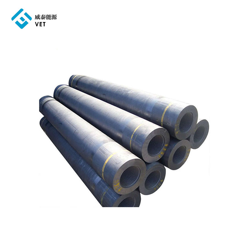
Graphite e...