Thin film deposition is to coat a layer of film on the main substrate material of the semiconductor. This film can be made of various materials, such as insulating compound silicon dioxide, semicon...
Detailed analysis of heating principle of graphite rod
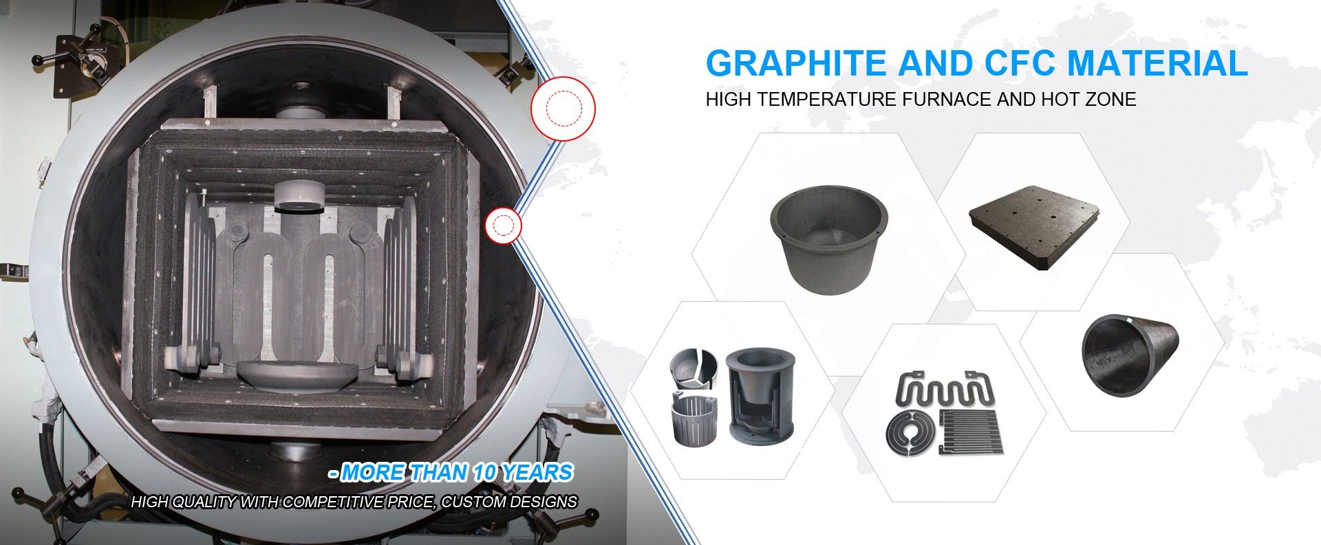
Graphite rod is often used as the electric heater of high-temperature vacuum furnace. It is easy to oxidize at high temperature. Except...
As semiconductor manufacturing continues to push toward higher temperatures, larger crystal sizes, and stricter process stability, the performance of structural materials inside thermal processing ...
Silicon carbide (SiC) is a new compound semiconductor material. Silicon carbide has a large band gap (about 3 times silicon), high critical field strength (about 10 times silicon), high thermal con...
1. Main processes of plasma enhanced chemical vapor deposition
Plasma enhanced chemical vapor deposition (PECVD) is a new technology for the growth of thin films by chemical reaction of gase...
Chemical vapor deposition (CVD) is the most widely used technology in the semiconductor industry for depositing a variety of materials, including a wide range of insulating materials, most metal ma...