Semiconductor manufacturing operates at the intersection of extreme precision and extreme environments. Processes such as epitaxy, crystal growth, and high-temperature annealing routinely exceed 1000°C, where even minor thermal fluctuations can translate into measurable variations in film thickness, dopant distribution, and ultimately device performance. In this context, materials that enable stable and repeatable thermal environments are not auxiliary—they are foundational.
Among these materials, graphite felt has emerged as a critical enabler of thermal management in advanced semiconductor processes. Often overlooked compared to wafers or deposition equipment, graphite insulation systems—particularly high-purity graphite felt for heat insulation—play a decisive role in maintaining process stability, improving yield, and supporting the transition toward wide-bandgap semiconductors such as SiC and GaN.
The Material Nature of Graphite Felt
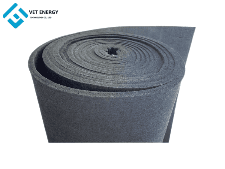
Graphite felt, sometimes referred to as carbon fiber felt, is a porous, lightweight material composed of entangled carbon fibers that have been heat-treated to achieve high purity and structural stability. Depending on processing methods, it can be supplied as soft insulation felt, rigid graphite felt, or graphite hard felt, each tailored for specific thermal and mechanical requirements.
What distinguishes graphite insulation felt from conventional insulation materials is its unique combination of properties. It exhibits extremely low thermal conductivity, enabling efficient heat retention even in ultra-high-temperature environments. At the same time, it maintains structural integrity at temperatures exceeding 2000°C in inert or reducing atmospheres. Its chemical inertness and low impurity levels—especially in semiconductor-grade materials—ensure minimal contamination risk, which is critical in front-end fabrication processes.
In advanced applications, high-purity graphite felt for heat insulation is further refined to reduce metallic impurities to ppm or even sub-ppm levels. This level of purity aligns with the stringent contamination control requirements of modern semiconductor fabs, particularly in processes involving compound semiconductors.
Applications in Key Semiconductor Processes
The most significant application of graphite felt lies in its ability to engineer and stabilize thermal fields across a wide range of high-temperature processes. In epitaxial growth, whether for silicon, silicon carbide, or gallium nitride, maintaining uniform temperature distribution across the wafer surface is essential. Graphite felt is typically integrated into the reactor as an insulating layer, wrapped around heating elements, or placed behind sensors. By minimizing radial and axial temperature gradients, it enables consistent growth rates and uniform material properties, directly impacting device performance and yield.
In silicon carbide epitaxy, where process temperatures can approach 1600°C, graphite insulation felt becomes indispensable. Its role extends beyond simple insulation; it actively shapes the thermal profile within the reactor, ensuring stable vapor-phase reactions and reducing thermal stress on wafers. Without such control, issues such as thickness non-uniformity, wafer warpage, and defect formation become significantly more pronounced.
Crystal growth processes further highlight the strategic importance of graphite felt. In methods such as physical vapor transport (PVT) for SiC or the Czochralski process for silicon, the thermal gradient within the growth chamber determines crystal quality. Here, rigid graphite felt or graphite hard felt is often employed to create controlled insulation zones. By adjusting felt density, thickness, and configuration, engineers can fine-tune heat flow, thereby influencing crystal growth rates, defect density, and overall boule quality. In SiC crystal growth, such thermal management directly correlates with the reduction of micropipes and dislocations.
Graphite felt also plays a supporting but critical role in chemical vapor deposition (CVD) and metal-organic chemical vapor deposition (MOCVD) systems. As a graphite insulation felt, it helps maintain a stable thermal environment within the reactor, reducing heat loss and mitigating cold-wall effects. This contributes to improved deposition uniformity and process repeatability, particularly in large-scale production environments.
In high-temperature annealing and diffusion processes, especially those associated with wide-bandgap semiconductors, graphite felt contributes to energy efficiency and thermal stability. By minimizing heat dissipation, it allows furnaces to maintain consistent temperatures with lower energy input, while also reducing thermal cycling stress on process components.
Beyond wafer fabrication, graphite felt is widely used in upstream material processing, including powder sintering, ceramic fabrication, and the purification of graphite components. These processes, while not always visible within the semiconductor fab, are essential for producing the high-performance materials that underpin advanced device manufacturing.
Trends: Toward Higher Purity and Functional Integration
As the semiconductor industry evolves toward more demanding applications—particularly in electric vehicles, renewable energy, and high-frequency electronics—the requirements placed on thermal management materials are becoming increasingly stringent. This trend is especially evident in the rapid adoption of SiC and GaN technologies, where higher operating temperatures and tighter process windows demand superior insulation performance.
One of the most significant developments is the push toward ultra-high-purity materials. High-purity graphite felt for heat insulation is being engineered with ever-lower impurity levels to meet the contamination standards of next-generation fabs. At the same time, structural innovations such as rigid graphite felt and graphite hard felt are enabling more precise thermal field control and longer service lifetimes.
Another important trend is the integration of protective coatings, such as silicon carbide (SiC), onto graphite felt surfaces. These coatings enhance oxidation resistance, reduce particle generation, and extend operational durability, addressing some of the traditional limitations of carbon-based insulation materials.
Looking ahead, graphite felt is expected to evolve from a passive insulation medium into a more actively engineered component of semiconductor equipment design. Through advanced material processing and customization, it will continue to support the industry’s pursuit of higher efficiency, greater reliability, and tighter process control.
Post time: Apr-17-2026