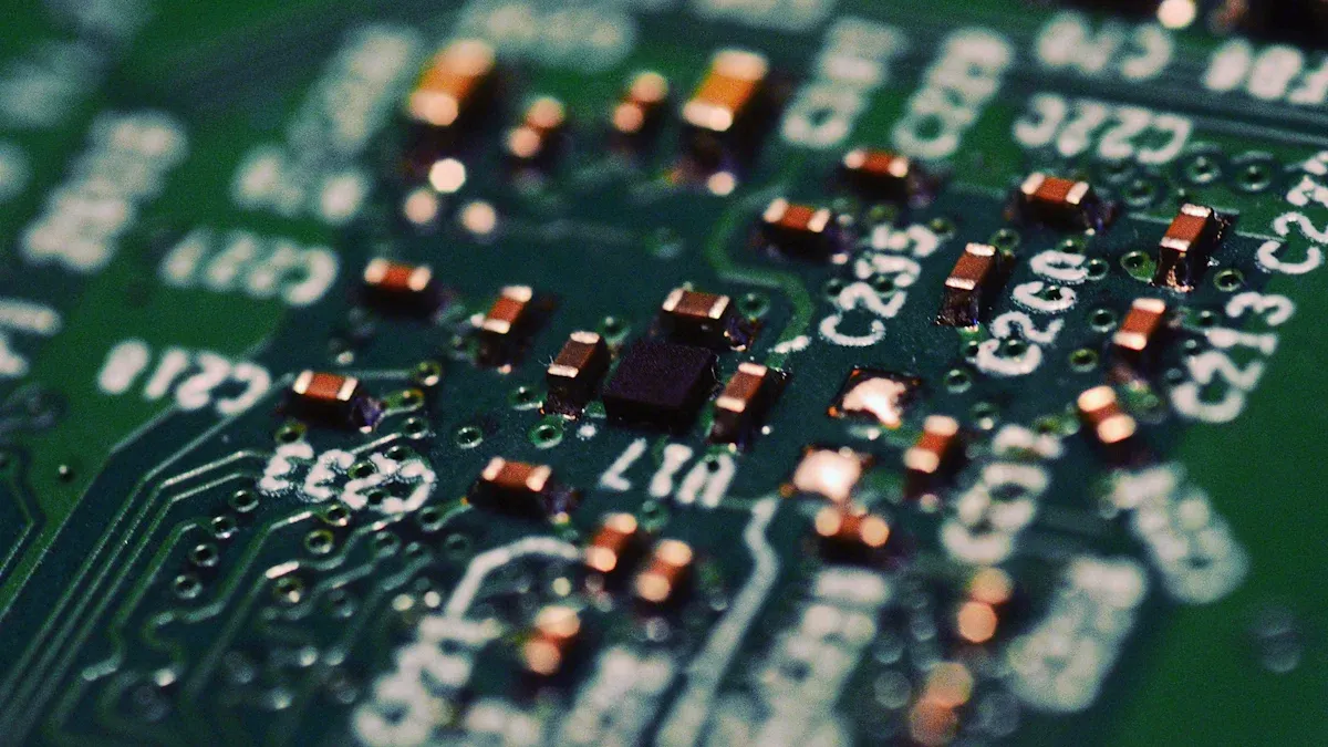
MOCVD is primarily used for growing thin semiconductor films. These films are essential for advanced electronic and optoelectronic devices. The market for MOCVD technology demonstrates robust growth. Experts estimate its market value at USD 1.1 billion in 2023. They forecast revenue to reach USD 2.8 billion by 2033, showing a compound annual growth rate (CAGR) of 9.7%. This significant expansion underscores MOCVD’s critical role in technological advancement.
Key Takeaways
- MOCVD grows thin semiconductor films. These films are important for many electronic devices.
- MOCVD helps make advanced devices. These include LEDs, laser diodes, and power electronics.
- MOCVD is good for renewable energy. It helps create better solar cells and light sensors.
- MOCVD offers great control. It builds layers with atomic precision for better device performance.
- MOCVD can make many devices at once. This makes it good for large-scale production.
MOCVD for Advanced Optoelectronic Devices
Metal-Organic Chemical Vapour Deposition (MOCVD) plays a pivotal role in the fabrication of advanced optoelectronic devices. This technology enables the precise growth of thin semiconductor films, which are fundamental to the performance of modern light-emitting diodes, laser diodes, and infrared emitters.
MOCVD in LED Manufacturing
This deposition technique is indispensable for manufacturing high-performance Light-Emitting Diodes (LEDs). It facilitates the growth of critical material systems such as Gallium Nitride (GaN), Gallium Arsenide (GaAs), and Indium Phosphide (InP), along with arsenide/phosphide (As/P) compounds. These materials form the basis for efficient light emission. For instance, high-performance 407 nm violet InGaN multi-quantum-wells LEDs are fabricated using this method. These devices often incorporate an un-doped GaN current spreading layer and AlGaN barriers with high aluminum content. This design improves light-emission efficiency by diminishing injection current overflow. InGaN/GaN multi-quantum wells (MQWs) represent a typical material composition for high-brightness LED fabrication. Growth using this technique significantly improves the uniformity and coverage of these atomically thin films, which directly impacts the wafer-scale synthesis of 2D materials for high-performance optoelectronic devices. A red InGaN LED, emitting at 625 nm, achieved a record external quantum efficiency (EQE) of 10.5% through a complex epitaxial procedure involving stacked superlattice layers and strain compensation.
MOCVD for Laser Diodes
Laser diodes, crucial components in optical communication and data storage, heavily rely on this technology. This method enables the growth of high-quality epitaxial films using material systems like Gallium Arsenide (GaAs), Gallium Nitride (GaN), and Indium Phosphide (InP). Growth techniques facilitate the development of visible wavelength laser diodes from III-V alloys such as InGaPAs and InGaAlP. Furthermore, InAs/GaAs quantum dot laser diodes grown by this technology emit O-band light, specifically at 1.3 µm. The precision of the deposition process contributes significantly to the reliability and lifespan of these devices. For example, it has been instrumental in growing high-quality epitaxial films for ZnSe-based laser diodes, leading to a significant improvement in their lifetime, reaching approximately 500 hours at 20°C under continuous wave operation. Researchers also utilize this method to grow broad-area strained InGaAs-AlGaAs single quantum well lasers operating at approximately 975nm, which helps in understanding degradation mechanisms.
MOCVD in Infrared Emitters
This deposition method is also vital for producing advanced infrared emitters, which find applications in sensing, imaging, and communication. The technique allows for the precise deposition of complex material structures. Mid-infrared lasers, for example, are grown using this process. These sophisticated devices incorporate AlAsSb claddings, strained InAsSb active regions, and multi-stage, type I InAsSb/InAsP quantum well active regions. They also feature semi-metal GaAsSb/InAs layers, which act as internal electron sources for multi-stage injection lasers, and AlAsSb serves as an electron confinement layer. These structures represent the first multi-stage devices grown by this method, showcasing the technology’s capability to create highly specialized infrared components. The ability to control uniformity and coverage of synthesized films is critical for the performance of these advanced infrared devices.
MOCVD in High-Performance Electronics
Metal-Organic Chemical Vapour Deposition (MOCVD) is a cornerstone technology for developing high-performance electronic devices. This technique enables the precise growth of semiconductor layers crucial for power electronics, high-frequency transistors, and advanced sensors.
MOCVD for Power Electronics
Power electronics demand materials capable of handling high power densities and extreme temperatures. MOCVD is vital for producing materials like Gallium Nitride (GaN) and Silicon Carbide (SiC), which possess superior thermal conductivity and high breakdown voltage. These properties are essential for modern power systems. Wide-bandgap semiconductors such as SiC and GaN are well-suited for demanding power environments. Devices are subjected to high voltage, current, and temperature in these settings. GaN diodes, for instance, fabricated with MOCVD-grown drift regions, have demonstrated breakdown voltages exceeding 1.3 kV. Twelve devices from a single wafer showed this capability, reaching approximately 90 percent of the theoretical parallel-plane limit.
MOCVD enables the growth of high-quality, single-crystal epitaxial layers on SiC substrates with low defect densities. This is crucial for power semiconductors. The process provides precise control over the thickness, doping concentration, and layer uniformity of the epitaxial layer. These factors optimize electrical properties essential for complex electronic devices. Furthermore, MOCVD is suitable for large-scale production. It allows for the growth of epitaxial layers on both small and large substrates, making SiC-based devices cost-effective for widespread adoption. III-nitride semiconductor materials, including GaN, AlGaN, InGaN, AlN, and InAlN, are grown via this method for high-performance applications in power electronics, photonics, and clean energy technologies. These materials are crucial for devices like high-efficiency power transistors (HEMTs), UV-visible LEDs, and laser diodes.
MOCVD in High-Frequency Transistors
High-frequency transistors, critical for advanced communication systems, also benefit significantly from MOCVD. The process facilitates the growth of InP-based material systems for devices such as High Electron Mobility Transistors (HEMTs), Heterojunction Bipolar Transistors (HBTs), PIN, Mixer, and Multiplier diodes. For example, researchers fabricate AlGaN/GaN High-Electron-Mobility Transistors (HEMTs) on 4-inch GaN on SiC substrates. The epitaxial wafer, grown by MOCVD, consists of an i-GaN buffer layer, a 0.9 μm unintentionally doped GaN channel layer, a 25 nm Al0.25Ga0.75N barrier layer, and a 2 nm GaN cap layer. Hall measurements at room temperature showed an electron mobility of 1500 cm²/V·s, a sheet resistance of 280 Ω/sq, and a sheet carrier density of 1 × 10¹³/cm².
Optimizing ohmic etching patterns (OEPs) for Ka-band applications further enhances performance. A 1 μm line pattern OEP demonstrated superior results compared to other patterns.
| Performance Metric | 1 μm Line OEP | Other OEPs (e.g., 1 μm holes, 3 μm holes, 3 μm lines) |
|---|---|---|
| Contact Resistance | Lowest | Higher |
| Small Signal Performance | Highest | Lower |
| Large Signal Performance | Highest | Lower |
| Minimum Noise Figure (NFmin) | Smallest | Larger |
| On-resistance (Ron) | 1.61 Ω·mm | Higher |
This optimized OEP structure, combined with the MOCVD-grown epitaxial layers, leads to improved radio frequency performance. It achieves this by reducing access resistance and increasing contact area.
MOCVD for Advanced Sensors
Advanced sensors rely on precisely engineered semiconductor layers for enhanced sensitivity and selectivity. MOCVD growth of 2D transition metal dichalcogenides (TMDs) like molybdenum disulfide (MoS2) is crucial for next-generation nano-electronic devices. These applications often include advanced sensing technologies, benefiting from the precise layer-by-layer growth and high crystallinity offered by the method.
MOCVD-grown ZnGa2O4 layers are highly beneficial for NO gas sensors. Research has shown that plasma surface treatment significantly enhances their performance. This leads to an 8-fold improvement in sensor response for 5 ppm NO gas concentration, reaching 1276.1%. This optimized sensor also achieved a low limit of detection of 2.4 ppb, demonstrating the effectiveness of the technique in producing high-performance NO gas sensors.
Furthermore, indium oxide nanowires and In2O3 thin films grown by this process demonstrate good selectivity to NO2. These materials show minimal interference from other gases, indicating improved selectivity. A ZnGa2O4 (ZGO) epilayer grown by MOCVD exhibited high sensitivity, reversibility, and selectivity for detecting NO at 300 °C. The ZGO sensor showed a sensitivity of 1.88 when exposed to 125 ppb NO. It demonstrated high sensitivity to NO while barely reacting with CO2, CO, and SO2, indicating enhanced selectivity. The ZGO sensor also showed a greater response to NO compared to NO2. First-principles simulations confirmed that the ZGO gas sensor’s strong response to NO is due to a significant change in work function upon NO molecule adsorption on the thin-film surface.
MOCVD for Renewable Energy and Detection
Metal-Organic Chemical Vapour Deposition (MOCVD) significantly contributes to advancements in renewable energy technologies and sophisticated detection systems. This technique enables the creation of high-performance materials crucial for efficient solar cells and sensitive photodetectors.
MOCVD in Multi-Junction Solar Cells
MOCVD is essential for producing high-efficiency solar panels. It enables the creation of compound semiconductors with improved energy conversion rates. This technology is crucial for generating more power from sunlight, aligning with the global emphasis on renewable energy. Researchers typically fabricate GaInP/GaInAs/Ge devices using MOCVD for commercial-scale production of high-efficiency multi-junction solar cells. These complex structures maximize sunlight absorption across different parts of the solar spectrum.
For example, a five-junction III-V solar cell, fabricated using MOCVD, achieved a power conversion efficiency of 35.1%. This 12 cm² device featured an AlGaInP-AlGaAs-GaAs-InGaAs-InGaAs structure. Each subcell had specific bandgap energies, allowing for optimal light capture. This precise layering capability makes MOCVD indispensable for pushing the boundaries of solar energy conversion.
MOCVD for Efficient Photodetectors
MOCVD also plays a critical role in fabricating efficient photodetectors. These devices convert light into electrical signals, finding applications in communication, imaging, and sensing. The technique allows for precise control over material composition and layer thickness, which directly influences a photodetector’s performance.
MOCVD facilitates the growth of InGaAs PIN photodetector membranes on InP substrates. Engineers can optimize the InGaAs photodetector’s spectral sensitivity for wavelengths within a broad range (0.4 μm-3.6 μm). This optimization occurs by precisely controlling material composition, such as In0.53Ga0.47As, which has a bandgap of 0.74 eV and covers key communication wavelengths. MOCVD allows for the precise deposition of various layers, including p- and n-type InP, and multiple InGaAs layers with specific thicknesses (e.g., a 2.2 μm undoped InGaAs absorption layer). These layers are crucial for defining the photodetector’s spectral response.
Furthermore, MOCVD enables the growth of (In1-xAlx)2O3 films with a tunable bandgap on MgO substrates. The bandgap tunability, influenced by chemical composition and growth temperature, directly enables the fabrication of photodetectors sensitive to specific spectral ranges. This precision extends to response speed as well. Photodetectors utilizing MOCVD-grown Ga2O3 films have demonstrated a response speed better than 0.1 seconds. Specifically, Schottky barrier photodiodes based on Ga2O3 on mica exhibited this rapid response, highlighting the technology’s capability for high-speed detection.
The Precision and Versatility of MOCVD
Metal-Organic Chemical Vapour Deposition offers unique advantages in semiconductor manufacturing. Its precision and versatility make it indispensable for creating advanced electronic and optoelectronic devices. This technology allows for exceptional control over material properties and layer structures.
MOCVD’s Role in Material Versatility
This deposition technique demonstrates remarkable material versatility. It deposits a wide range of materials. These include II-VI materials, III-V materials, and high-purity crystalline compound semiconducting thin films. It also forms micro/nanostructures, 0D, 1D, and 2D nanomaterials. Specifically, it excels with III-V semiconductors, involving metallic elements like gallium and indium, and group V elements such as arsenic and phosphorus. GaAs heterostructures and GaN-based materials for LEDs and electronic devices are common applications.
This is a highly versatile technique. It deposits compound semiconductors, nitrides, and oxides by varying precursor chemistry. It is typically preferred for phosphide (P) materials. For arsenide-based materials, this technique and MBE have similar capabilities. However, MBE is the preferred method for antimonide (Sb) material growth and for more advanced structures like quantum dots.
| Technique | Material Versatility |
|---|---|
| MOCVD | Creates complex, high-purity crystalline structures with exceptional control. |
| General CVD | More scalable and cost-effective for a wider range of simpler materials. |
MOCVD for Precise Layer Control
The technique enables the growth of complex heterostructures with atomic-level precision. Engineers create atomically sharp transitions between layers. This happens by simply switching the precursor gases flowing into the reactor. This control is crucial for tailoring the electronic and optical properties of multi-layered semiconductor devices. The process is considered ‘atomic-level construction’. Ultra-thin, crystalline layers are built atom by atom. This highly controlled method facilitates epitaxial growth. Atoms arrange themselves in a highly ordered fashion, mirroring the underlying crystal structure of the wafer. This ensures a layer-by-layer continuation of the crystal structure.
MOCVD’s Scalability for Production
This system also offers significant scalability for high-volume production. Industrial reactors accommodate multiple wafers. Planetary Reactors, for example, handle wafers up to 200 mm (approximately 8 inches). This supports low-cost, high-volume manufacturing. A fifth-generation GaN Planetary Reactor grew eight 6-inch epiwafers in a single run.
- 4-inch wafers are widely used for balancing cost and volume in high-volume production.
- 6-inch wafers are gaining traction for high-volume manufacturing, despite technical challenges.
MOCVD is indispensable for fabricating a wide array of modern electronic and optoelectronic devices. Its unique capabilities in precision and material versatility drive innovation across numerous high-tech industries. This technology enables the creation of complex semiconductor structures with exceptional control. MOCVD continues as a cornerstone technology, enabling advancements in lighting, communication, computing, and renewable energy. It consistently pushes the boundaries of what is possible in advanced material science.
Post time: Nov-13-2025