TaC coating is critical for GaN and SiC device production. It provides superior protection against corrosive process environments, enhances thermal stability, and prevents contamination. These factors are essential for achieving high device performance and yield. The Asia-Pacific GaN power device market projects a 19.33% Compound Annual Growth Rate between 2025 and 2032. The overall market for these devices, valued at USD 2.24 billion in 2023, anticipates reaching USD 18 billion by 2032, growing at a 25% CAGR. This significant market expansion underscores the need for robust manufacturing solutions.
Key Takeaways
- TaC coating protects equipment used to make GaN and SiC devices. It stops damage from harsh chemicals and high heat.
- GaN and SiC devices are better than old silicon devices. They work faster and use less power, but they are hard to make.
- TaC coating helps make GaN and SiC devices cleaner. It stops tiny bits of dirt from getting into the devices.
- TaC coating makes sure devices are made the same way every time. This means more good devices are made and fewer are wasted.
- TaC coating is very important for making new power electronics. It helps these advanced devices work well and last longer.
GaN and SiC Devices: The Next Generation of Power Electronics

Overview of GaN and SiC Device Advantages
Gallium Nitride (GaN) and Silicon Carbide (SiC) devices represent a significant leap forward in power electronics. They offer substantial improvements over traditional silicon-based components. SiC devices, for example, demonstrate superior characteristics across several critical parameters:
| Parameter | SiC | Silicon (Si) | Advantage |
|---|---|---|---|
| Bandgap | 3.2 eV | 1.1 eV | 3x higher |
| On-resistance (RDS(on)) | Up to 10x lower | Higher | Reduced conduction losses |
| Switching Speed | 10-100x faster | Slower | Minimized transient losses |
| Max Junction Temp | 200–250°C | 125–150°C | 2x higher operational range |
| Thermal Conductivity | 3.7 W/cm·K | 1.5 W/cm·K | 2.5x better heat dissipation |
| Breakdown Field | 3 MV/cm | 0.3 MV/cm | 10x higher voltage blocking |
SiC devices achieve higher efficiency and lower power losses. They reduce both conduction and switching losses. SiC’s bandgap is three times higher than silicon’s, allowing for thinner drift layers. This reduces on-resistance by up to ten times for the same voltage rating. A 1200V SiC MOSFET has five times lower conduction loss than a silicon IGBT. SiC devices also switch 10 to 100 times faster than silicon, minimizing transient losses. SiC Schottky diodes eliminate reverse recovery, removing a major source of loss. These devices operate at higher temperatures, with a maximum junction temperature of 200–250°C, twice that of silicon. They also possess 2.5 times better thermal conductivity, enhancing heat dissipation. SiC’s strong atomic bonds resist electromigration and gate oxide breakdown, contributing to a longer lifespan.
Manufacturing Challenges for GaN and SiC Devices
Producing GaN and SiC devices presents unique manufacturing challenges. These challenges stem from the materials’ inherent properties and the complex fabrication processes.
For GaN devices, manufacturers face several hurdles:
- Crystal Quality and Defect Density: Achieving high crystal quality with low defect density is difficult. GaN often grows on substrates like sapphire or silicon, which have different lattice constants. This mismatch creates defects during epitaxial growth, impacting device performance.
- Epitaxial Growth Processes: Methods like Metal-Organic Chemical Vapor Deposition (MOCVD) are costly and require precise control. Hydride Vapor Phase Epitaxy (HVPE) offers faster growth but complicates gas-phase reactions and surface quality.
- Doping and Uniformity: Achieving uniform doping levels, especially for p-type GaN, is challenging. This is due to the material’s properties and complex chemical processes.
- Substrate Availability and Cost: The availability and cost of substrates affect GaN scalability. Silicon substrates are cheaper but introduce greater lattice mismatches.
SiC device production also encounters significant difficulties:
- Extreme Hardness and Brittleness: SiC’s hardness (Mohs 9) and brittleness complicate manufacturing. Wafer polishing is slow and inefficient, requiring specialized slurries.
- Wafer Handling: Handling SiC wafers is difficult due to their brittleness. This leads to chipping, cracking, and particle contamination.
- Epitaxy Requirements: Epitaxy for SiC requires higher temperatures than silicon. This shortens the lifespan of chamber components and increases maintenance costs.
- Ion Implantation: Aluminum implantation for p-type doping faces ion source stability issues. Dopants do not diffuse easily and can form craters. High annealing temperatures (1800°C) can carbonize the surface.
The Core Problem: Material Degradation and Contamination in Processing
Equipment Corrosion and Erosion in Harsh Environments
Semiconductor manufacturing equipment faces significant material degradation and wear. Harsh environments, including exposure to corrosive chemicals and abrasive processes, cause these issues. This leads to reduced equipment lifespan and compromised production efficiency. Etching and deposition tools, in particular, endure extreme conditions. They encounter plasma, high temperatures, and reactive chemicals. These factors result in erosion and chemical attack. Such conditions collectively contribute to equipment failure by degrading materials and reducing tool performance.
A “corrosion-wear coupled failure mechanism” often occurs. Corrosive media weakens grain boundary bonding strength. This weakening allows friction-induced fatigue cracks to spread rapidly. These cracks propagate along tin-enriched phase aggregation zones. This composite damage mode proves challenging to suppress with traditional surface coating technologies, especially in severe corrosion-friction environments.
Impact of Contamination on GaN and SiC Device Performance
Contamination severely impacts the performance and yield of GaN and SiC devices. Even minute impurities can create defects, leading to device malfunction or reduced efficiency. For GaN devices, specific contaminants frequently cause problems:
- Deep electron traps (E2 and E4): These traps increase after proton and electron irradiation. They cause gate and drain-lag phenomena, contributing to current collapse and degradation in AlGaN/GaN HEMTs.
- Dislocations: Open-core screw dislocations promote gate leakage in AlGaN/GaN HEMTs. Dislocations decorated by Indium (In) affect InAlN/GaN HEMTs. They also link to deep electron traps, trapping, subthreshold current leakage, and overall degradation.
- Gallium vacancies complexed with Silicon (Si) or Oxygen (O): These complexes act as major hole traps in n-GaN and n-AlGaN.
- Carbon (C): Carbon also functions as a major hole trap in n-GaN and n-AlGaN.
- Hydrogen: This background impurity, common in MOCVD and NH3-rich MBE grown materials, influences threshold voltage shifts and transconductance degradation under proton irradiation.
- Deep acceptors: The introduction of deep acceptors in the barrier layer explains changes in threshold voltage and channel mobility in AlGaN/GaN transistors.
- Deep traps in GaN buffer layer: These traps can lead to similar effects as deep acceptors. They contribute to partial 2DEG depletion and 2DEG electron scattering.
How TaC Coating Addresses Critical Manufacturing Challenges
Exceptional Chemical Inertness of TaC Coating
TaC coating offers exceptional chemical inertness. This property makes it highly valuable in semiconductor manufacturing. It effectively resists erosion from corrosive gases like chlorides and fluorides. The coating maintains low reactivity in high-temperature environments. This prevents unwanted chemical reactions with reactive gases. This characteristic is crucial for ensuring process purity and high-quality material deposition. It particularly benefits applications involving Silicon Carbide Wafer Boats and other key components.
“Compared with SiC coating, TaC has higher chemical inertness and corrosion resistance.”
TaC coatings resist hot ammonia. They also resist hydrogen vapors, silicon vapors, and molten metals. These coatings provide protection against H2, NH3, SiH4, and Si in harsh chemical environments.
High Thermal Stability and Mechanical Hardness of TaC Coating
High thermal stability and mechanical hardness are critical for components in GaN and SiC production. TaC-coated graphite demonstrates superior chemical corrosion resistance compared to bare graphite or SiC-coated graphite. It remains stable at high temperatures, reaching 2600°C. It does not react with numerous metal elements. This makes it the preferred coating for third-generation semiconductor single crystal growth and wafer etching. It is particularly useful for MOCVD equipment in GaN or AlN single crystal growth and PVT equipment in SiC single crystal growth. This significantly enhances crystal quality.
Tantalum Carbide (TaC) coatings can be stably used at high temperatures up to 2600°C. They do not react with many metallic elements. This coating is considered optimal for third-generation semiconductor single crystal growth and wafer etching. Specifically, it benefits MOCVD equipment growth of GaN or AlN single crystals and PVT equipment growth of SiC single crystals.
The mechanical hardness of this material also contributes to its durability. It has a Vickers hardness of approximately 1,880 HV.
| Coating Type | Vickers Hardness (HV) |
|---|---|
| Tantalum carbide (TaC) | 1600 to 1800 |
| Titanium carbide (TiC) | 3200 |
| Boron carbide (B4C) | 3400 to 3700 |
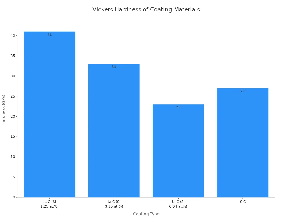
| Coating Type | Hardness (GPa) |
|---|---|
| ta-C (Si 1.25 at.%) | 41 |
| ta-C (Si 3.85 at.%) | 33 |
| ta-C (Si 6.04 at.%) | 23 |
| SiC | 27 |
Ultra-High Purity and Low Particle Generation with TaC Coating
Maintaining ultra-high purity and minimizing particle generation are paramount in semiconductor manufacturing. CVD TaC coated carriers are noted for their extremely low particle generation rates. Their smooth surface characteristics significantly reduce the potential for particle contamination. This, in turn, helps to improve purity and yield during epitaxial growth processes.
Improved Process Repeatability and Yield with TaC Coating
TaC coating significantly enhances process repeatability in GaN and SiC device manufacturing. The coating’s exceptional durability and resistance to harsh processing environments ensure that reactor components maintain their integrity and surface characteristics over extended operational periods. This consistency is crucial for achieving uniform film deposition, precise doping profiles, and stable thermal conditions across multiple production runs. When equipment surfaces remain stable and free from degradation, manufacturers can reliably reproduce desired process parameters. This predictability minimizes variations in device characteristics from wafer to wafer and batch to batch.
This improved repeatability directly translates into higher manufacturing yields. A stable process environment reduces the incidence of defects caused by material degradation, contamination, or inconsistent processing conditions. For instance, the chemical inertness of TaC coating prevents unwanted reactions between process gases and reactor walls, which could otherwise introduce impurities or alter gas flow dynamics. Its high thermal stability ensures components do not warp or degrade under extreme temperatures, maintaining precise geometries essential for uniform growth. Furthermore, the ultra-high purity and low particle generation associated with TaC coating drastically reduce particulate contamination, a major cause of device failures. By mitigating these common sources of variability and defects, manufacturers produce a greater number of functional GaN and SiC devices per wafer, optimizing overall production efficiency and reducing waste.
Key Applications of TaC Coating in GaN and SiC Production
TaC Coating for Reactor Components
TaC coating plays a crucial role in protecting various reactor components within GaN and SiC production. Specific components benefiting from this advanced coating include wafer carriers, injectors, susceptors, and heaters. In SiC CVD reactors, critical components coated with Tantalum Carbide demonstrate significant performance improvements. This coating stands out for its extreme hardness and metallic conductivity. It offers exceptional resistance to halogen and hydrogen corrosion, making it ideal for harsh plasma and high-temperature environments.
The coating also provides high thermal conductivity, effectively dissipating heat and preventing localized overheating during high-temperature processes. It protects critical furnace and reactor components at temperatures up to 2200°C, maintaining chemical and mechanical stability. Tantalum carbide has strong corrosion resistance to most acids and alkalis, preventing substrate damage in corrosive environments. It resists hydrogen, ammonia, monosilane, and silicon, providing protection in harsh chemical settings. This enhanced protection leads to an extended component lifespan. TaC coating also boasts ultra-high purity, with impurity levels often below 5 ppm. This significantly reduces defects like micropores and etch pits in SiC crystals, improving crystal quality.
TaC Coating for Etch Chambers and Plasma Processing Equipment
TaC coating is equally vital for etch chambers and plasma processing equipment. Its exceptional hardness and chemical inertness resist wear and corrosion from abrasive plasma environments and harsh chemical reactions. This ensures components remain functional under extreme conditions. The ultra-high purity of the coating, with impurity levels below 5 ppm, minimizes contamination risks in crystal growth processes.
Strong adhesion and low thermal expansion prevent cracking or delamination during thermal cycling. This is crucial for maintaining precision and consistency in semiconductor fabrication. In GaN/SiC epitaxial growth, the coating prevents gas reactions and minimizes defects, improving overall yield. High-purity materials and the durable TaC coating minimize particle generation and outgassing. This reduces the risk of wafer contamination and defects. The robust coating provides excellent resistance to plasma erosion and chemical attack, extending the operational life of components.
TaC coating is not merely beneficial; it is critical for enabling reliable, high-performance, and cost-effective production of GaN and SiC devices. It mitigates contamination and degradation challenges inherent in their manufacturing processes. Its role will only grow as these advanced technologies continue to develop. This ensures sustained innovation and market expansion.
FAQ
What is TaC coating?
TaC coating is a protective layer of Tantalum Carbide applied to graphite components. Manufacturers use a Chemical Vapor Deposition (CVD) process. This hard, refractory ceramic compound enhances stability and chemical resistance for semiconductor applications.
How does TaC coating improve manufacturing yield?
TaC coating ensures consistent process conditions. It prevents material degradation and contamination. This stability reduces defects and variations in device characteristics. Manufacturers achieve a higher number of functional GaN and SiC devices per wafer.
Why is TaC coating preferred over SiC coating in some applications?
TaC coating offers superior chemical inertness and corrosion resistance compared to SiC coating. It withstands harsher chemical environments and higher temperatures. This makes it more suitable for specific demanding processes in GaN and SiC production.
What specific components benefit from TaC coating in GaN/SiC production?
Reactor components like wafer carriers, injectors, susceptors, and heaters benefit significantly. Etch chambers and plasma processing equipment also utilize TaC coating. It protects these parts from corrosive gases, high temperatures, and abrasive plasma.
Take the Next Step
Ready to bring unprecedented stability and yield to your GaN and SiC processes?
Contact our material science experts today to discuss how a TaC coating solution can revolutionize your MOCVD or CVD reactor performance.
Post time: Nov-14-2025