SILICON WAFER
from sitronic
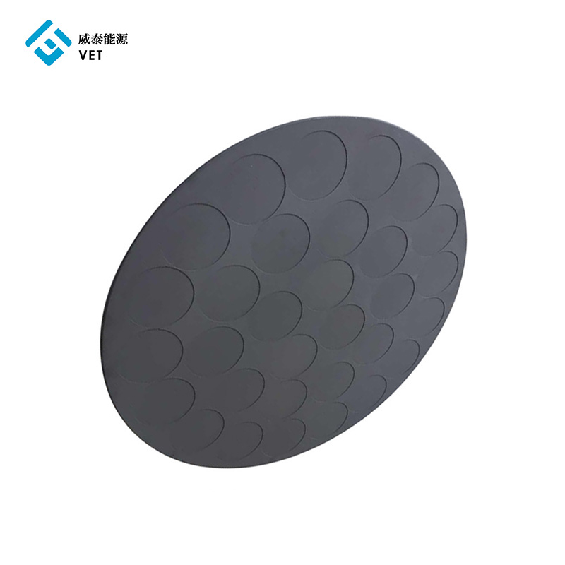
A wafer is a slice of silicon roughly 1 millimeter thick that has an extremely flat surface thanks to procedures that are technically very demanding. The subsequent use determines which crystal growing procedure should be employed. In the Czochralski process, for example, the polycrystalline silicon is melted and a pencil-thin seed crystal is dipped into the molten silicon. The seed crystal is then rotated and slowly pulled upwards. A very heavy colossus, a monocrystal, results. It is possible to select the monocrystal’s electrical characteristics by adding small units of high-purity dopants. The crystals are doped in accordance with the customer specifications and then polished and cut into slices. After various additional production steps, the customer receives its specified wafers in special packaging, which allows the customer to use the wafer immediately in its production line.
Today, a large portion of the silicon monocrystals are grown according to the Czochralski process, which involves melting polycrystalline high-purity silicon in a hyperpure quartz crucible and adding the dopant (usually B, P, As, Sb). A thin, monocrystalline seed crystal is dipped into the molten silicon. A large CZ crystal then develops from this thin crystal. Precise regulation of the molten silicon temperature and flow, the crystal and crucible rotation, as well as the crystal pulling speed results in an extremely high quality monocrystalline silicon ingot.
Post time: Jun-03-2021