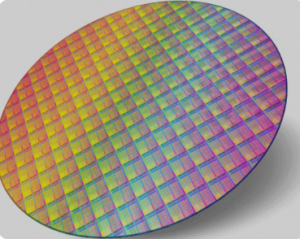
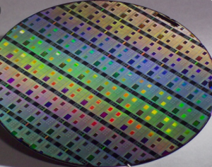
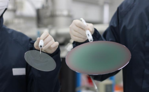
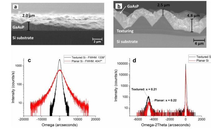
Gallium arsenide-phosphide epitaxial structures ,similar to produced structures of the substrate ASP type (ET0.032.512TU), for the. manufacture of planar red LED crystals.
Basic technical parameter
to gallium arsenide-phosphide structures
| 1,SubstrateGaAs | |
| a. Conductivitytype | electronic |
| b. Resistivity, ohm-cm | 0,008 |
| c. Crystal-latticeorientation | (100) |
| d. Surface misorientation | (1−3)° |
| 2. Epitaxial layer GaAs1-х Pх | |
| a. Conductivitytype |
electronic
|
|
b. Phosphorus content in the transition layer
|
from х = 0 to х ≈ 0,4 |
| c. Phosphorus content in a layer of constant composition |
х ≈ 0,4
|
| d. Carrier concentration, сm3 |
(0,2−3,0)·1017
|
| e. Wavelength at maximum of photoluminescence spectrum, nm | 645−673 nm |
| f. Wavelength at the maximum of the electroluminescence spectrum |
650−675 nm
|
| g. Constant layer thickness, micron |
At least 8 nm
|
| h. Layerthickness (total), micron |
At least30 nm
|
| 3 Plate with epitaxial layer | |
| a. Deflection, micron | At most 100 um |
| b. Thickness, micron | 360−600 um |
| c. Squarecentimetre |
At least 6 cm2
|
|
d. Specific luminous intensity (after diffusionZn), cd/amp
|
At least 0,05 cd/amp |


