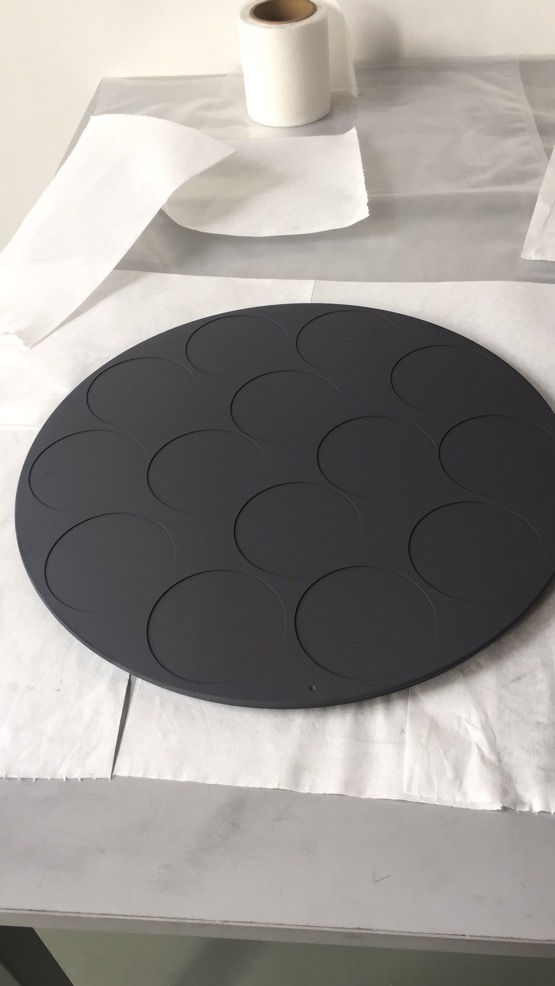
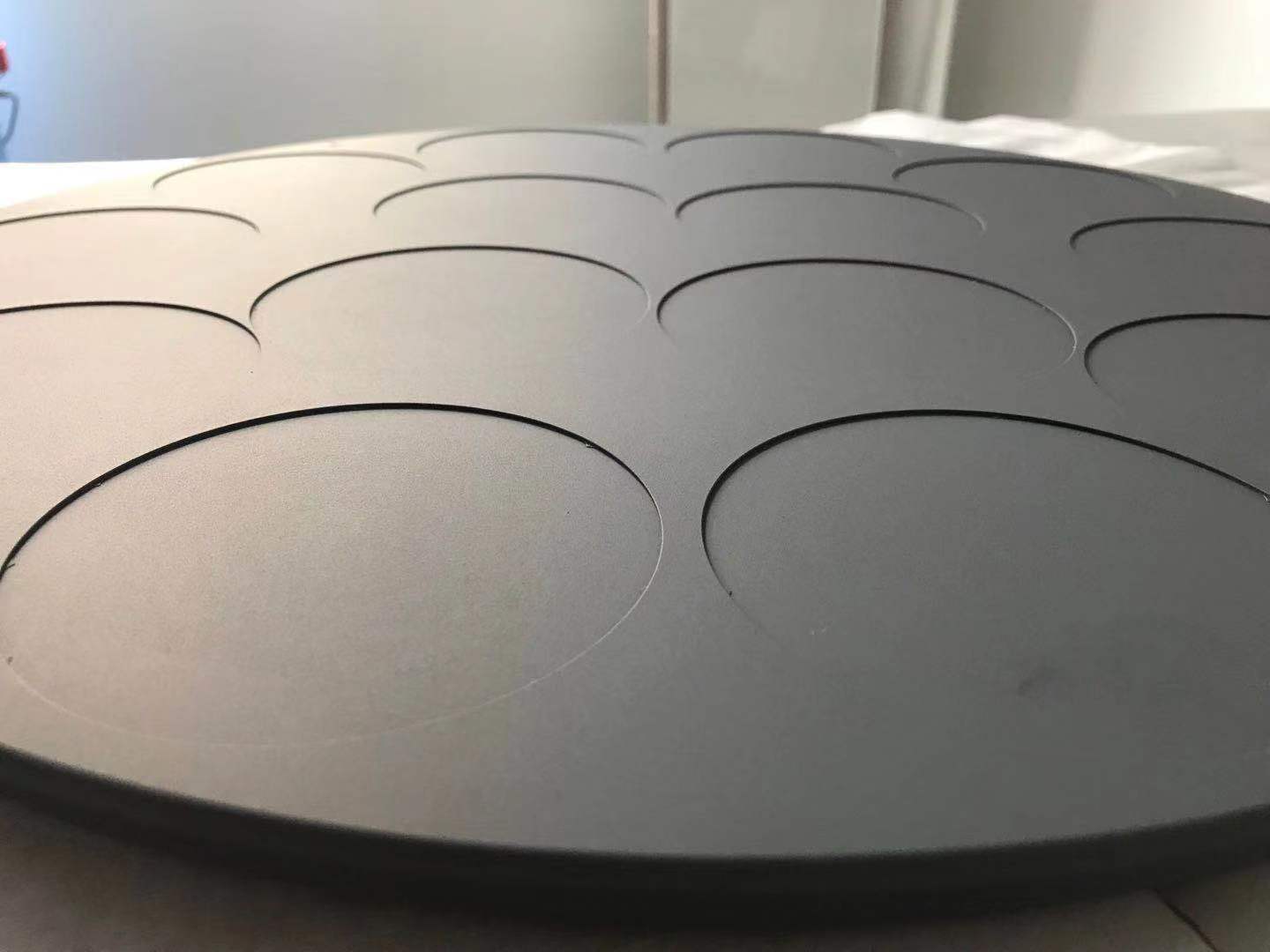
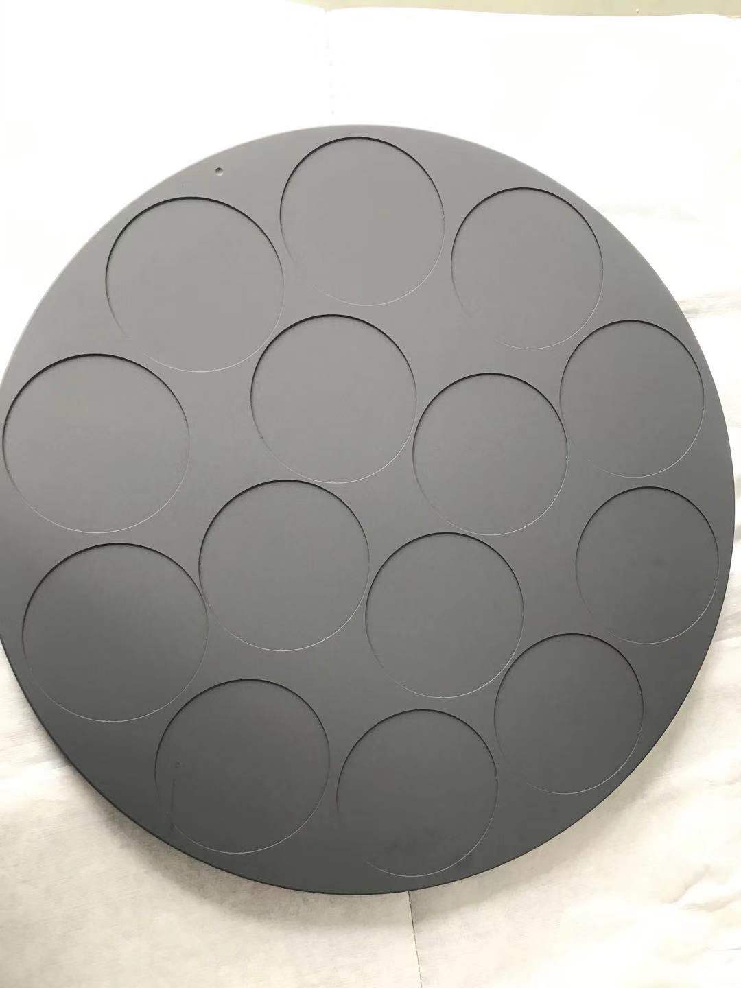
High-purity graphite components are crucial to processes in the semiconductor, LED and solar industry. Our offering ranges from graphite consumables for crystal growing hot zones (heaters, crucible susceptors, insulation), to high-precision graphite components for wafer processing equipment, such as silicon carbide coated graphite susceptors for Epitaxy or MOCVD. This is where our specialty graphite comes into play: isostatic graphite is fundamental for the production of compound semiconductor layers.These are generated in the “hot zone“ under extreme temperatures during the so-called epitaxy, or MOCVD process. The rotating carrier on which the wafers are coated in the reactor, consists of silicon carbide-coated isostatic graphite. Only this very pure, homogeneous graphite meets the high requirements in the coating process.
The basic principle of LED epitaxial wafer growth is: on a substrate (mainly sapphire, SiC and Si) heated to an appropriate temperature, the gaseous material InGaAlP is transported to the substrate surface in a controlled manner to grow a specific single crystal film. At present, the growth technology of LED epitaxial wafer mainly adopts organic metal chemical vapor deposition.
LED epitaxial substrate material is the cornerstone of the technological development of semiconductor lighting industry. Different substrate materials need different LED epitaxial wafer growth technology, chip processing technology and device packaging technology. Substrate materials determine the development route of semiconductor lighting technology.
Characteristics of LED epitaxial wafer substrate material selection:
1. The epitaxial material has the same or similar crystal structure with the substrate, small lattice constant mismatch, good crystallinity and low defect density
2. Good interface characteristics, conducive to the nucleation of epitaxial materials and strong adhesion
3. It has good chemical stability and is not easy to decompose and corrode in the temperature and atmosphere of epitaxial growth
4. Good thermal performance, including good thermal conductivity and low thermal mismatch
5. Good conductivity, can be made into upper and lower structure 6, good optical performance, and the light emitted by the fabricated device is less absorbed by the substrate
7. Good mechanical properties and easy processing of devices, including thinning, polishing and cutting
8. Low price.
9. Large size. Generally, the diameter shall not be less than 2 inches.
10. It is easy to obtain regular shape substrate (unless there are other special requirements), and the substrate shape similar to the tray hole of epitaxial equipment is not easy to form irregular eddy current, so as to affect the epitaxial quality.
11. On the premise of not affecting the epitaxial quality, the machinability of the substrate shall meet the requirements of subsequent chip and packaging processing as far as possible.
It is very difficult for the selection of substrate to meet the above eleven aspects at the same time. Therefore, at present, we can only adapt to the R & D and production of semiconductor light-emitting devices on different substrates through the change of epitaxial growth technology and the adjustment of device processing technology. There are many substrate materials for gallium nitride research, but there are only two substrates that can be used for production, namely sapphire Al2O3 and silicon carbide SiC substrates.
Post time: Feb-28-2022