Sputtering targets are mainly used in the electronics and information industries, such as integrated circuits, information storage, liquid crystal displays, laser memories, electronic control devices, etc. They can also be used in the field of glass coating, as well as in wear-resistant materials, high-temperature corrosion resistance , high-end decorative products and other industries.
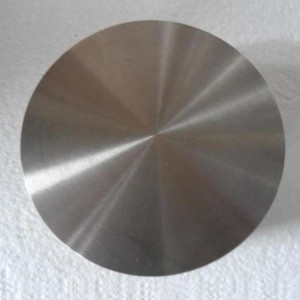
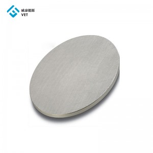
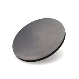
Sputtering is one of the main techniques for preparing thin film materials. It uses ions generated by ion sources to accelerate and aggregate in a vacuum to form high-speed energy ion beams, bombard the solid surface, and exchange kinetic energy between ions and solid surface atoms. The atoms on the solid surface leave the solid and are deposited on the surface of the substrate. The bombarded solid is the raw material for depositing thin films by sputtering, which is called sputtering target. Various types of sputtered thin film materials have been widely used in semiconductor integrated circuits, recording media, flat-panel displays and workpiece surface coatings.
Among all application industries, the semiconductor industry has the most stringent quality requirements for target sputtering films.High-purity metal sputtering targets are mainly used in wafer manufacturing and advanced packaging processes. Taking chip manufacturing as an example, we can see that from a silicon wafer to a chip, it needs to go through 7 major production processes, namely diffusion (Thermal Process), Photo-lithography (Photo-lithography), Etch (Etch), Ion Implantation (IonImplant), Thin Film Growth (Dielectric Deposition), Chemical Mechanical Polishing (CMP), Metalization (Metalization) The processes correspond one by one. The sputtering target is used in the process of “metallization”. The target is bombarded with high-energy particles by thin film deposition equipment and then a metal layer with specific functions is formed on the silicon wafer, such as conductive layer, barrier layer. Wait.Since the processes of the entire semiconductors are varied then some occasional situations are needed for verifying the system is existed correctly so we demand some kinds of dummy materials at certain stages of production to confirm the effects.
Post time: Jan-17-2022