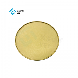
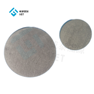
The CVD Coating Focus Ring for Plasma Etching is a critical consumable component used in advanced semiconductor etching systems. Engineered with a composite structure of substrate + CVD coating, this product is designed to optimize plasma distribution, improve etching uniformity, and extend chamber component lifetime.
At Vet Energy, we leverage deep expertise in chemical vapor deposition (CVD) technology and advanced ceramic materials to deliver focus rings that meet the stringent requirements of modern semiconductor nodes, including FinFET and 3D NAND processes.
Role of Focus Ring in Plasma Etching
In plasma etching systems (such as ICP and CCP reactors), the focus ring is positioned around the wafer edge and plays a vital role in process stability and yield performance.
1. Plasma Uniformity Control
The focus ring acts as an electrical and physical boundary that helps regulate plasma density distribution across the wafer surface.
Key benefits:
● Improved etch rate uniformity
● Reduced center-to-edge variation
● Enhanced process repeatability
2. Edge Effect Compensation
Without a focus ring, plasma sheath distortion at the wafer edge can lead to non-uniform etching.
The focus ring effectively functions as a “virtual wafer extension”, minimizing edge-related anomalies such as:
● Over-etching at wafer edges
● Critical dimension (CD) deviation
● Profile distortion
3. Ion Trajectory and Energy Control
By influencing the local electric field, the focus ring helps stabilize ion incident angles and energy distribution, which is crucial for:
● High aspect ratio (HAR) etching
● Anisotropic profile control
● Reduced sidewall damage
4. Chamber Protection and Contamination Reduction
As a sacrificial component, the focus ring absorbs direct plasma exposure and deposition byproducts.
Resulting advantages:
● Reduced chamber wall erosion
● Lower particle contamination
● Extended maintenance cycles (PM intervals)