
Core Summary: In semiconductor manufacturing, ppb-level boron contamination from graphite boats can ruin entire crystal growth runs. Learn how to specify and verify purity.
The Hidden Danger: Why “High Purity” Isn‘t Enough
Key takeaway: Ash content is not a sufficient purity specification for semiconductor applications. Elemental analysis — specifically for boron — is required to verify that a graphite boat won‘t contaminate the process.
In the graphite industry, “high purity” typically means low ash content. A graphite grade with ash content below 0.1% is considered high purity. Below 50 ppm, it‘s semiconductor grade. Below 5 ppm, it‘s ultra-high purity.
But here‘s the problem: ash content measures the total weight of non-carbon residue after burning. It doesn‘t tell you which elements are present. A graphite sample with 5 ppm ash that‘s mostly boron is a completely different material than one with 20 ppm ash that‘s mostly silicon. For semiconductor applications, the specific elements matter more than the total.
And the most problematic element in semiconductor graphite is boron. Boron acts as a p-type dopant in silicon and silicon carbide. Even at ppb concentrations, it shifts the electrical properties of the crystal. In SiC crystal growth, where the entire boule must meet precise doping specifications, boron contamination at the wrong level can render the material unusable.
The Boron Contamination Case: When 100 ppb Ruins a Crystal
Key takeaway: Boron contamination at the 100 ppb level can ruin an entire SiC crystal growth run. The financial impact of one failed run justifies the cost of rigorous incoming material verification.
The numbers involved in semiconductor crystal growth are unforgiving. Here‘s a case that shows why.
A SiC crystal growth furnace was using graphite components with a boron content of approximately 100 ppb — well within the specification for most industrial graphite grades, and even within some semiconductor-grade specifications. During crystal growth at 2300°C, boron diffused from the graphite into the SiC vapor phase and incorporated into the growing crystal.
The result was a p-type doping shift that made the entire boule unsuitable for power device applications. The boule was worth tens of thousands of dollars, and the entire growth run — 80 hours of furnace time — was wasted. The root cause wasn‘t a process error. It was a specification that looked clean on paper but contained an element that mattered at a concentration no one had measured.
This is why the semiconductor industry treats graphite purity differently from other sectors. As one patent notes, even the lowest-ash graphite commercially available typically contains boron above 0.2 ppm — and in some cases up to 1 ppm. For SiC crystal growth, that‘s already too high.
Beyond Ash Content: What to Look For
Key takeaway: The elements that matter depend on the process. For SiC growth, focus on boron and aluminum. For silicon epitaxy, focus on transition metals. But in all semiconductor applications, require elemental analysis, not just ash content.
When specifying a semiconductor-grade graphite boat, here are the elements that matter most and why.
Table 1: Critical Elements in Semiconductor Graphite Purity
| Element | Typical Specification | Impact on Semiconductor Process |
|---|---|---|
| Boron (B) | ≤0.1 ppm (100 ppb) | p-type dopant; shifts crystal doping |
| Aluminum (Al) | ≤0.1 ppm | p-type dopant; similar to boron |
| Iron (Fe) | <1 ppm | Deep-level trap; reduces carrier lifetime |
| Copper (Cu) | <1 ppm | Contamination; degrades device performance |
| Total metallic | <20 ppm | Overall contamination limit |
| Ash content | ≤50 ppm | Total residue; insufficient alone |
Data compiled from SEMI C-001 and semiconductor tool OEM specifications.
The SEMI C-001 standard provides the framework, but individual tool OEMs often have stricter requirements. For SiC crystal growth, the critical elements are boron and aluminum, both of which act as p-type dopants. For silicon epitaxy, transition metals like iron and copper are the primary concern because they create deep-level traps that reduce carrier lifetime.
Analytical Methods: ICP-MS and GDMS
Key takeaway: ICP-MS and GDMS are the two analytical methods for verifying ppb-level purity. GDMS is particularly important for boron analysis because boron can be lost during ICP-MS sample preparation.
Verifying ppb-level purity requires analytical methods that can detect and quantify specific elements at very low concentrations. The two methods used in the semiconductor industry are ICP-MS and GDMS.
ICP-MS (Inductively Coupled Plasma Mass Spectrometry) dissolves the graphite sample in acid and analyzes the resulting solution. It can detect most elements at ppb levels, making it suitable for boron, aluminum, and transition metal analysis. The sample preparation step — dissolving graphite without introducing contamination — is the most challenging part.
GDMS (Glow Discharge Mass Spectrometry) analyzes the solid graphite sample directly, without acid digestion. It‘s particularly useful for boron analysis because boron is difficult to keep in solution during ICP-MS sample preparation. GDMS also provides a full elemental survey, which is useful for screening unknown impurities.
For semiconductor-grade graphite boats, the standard practice is to require both ICP-MS and GDMS reports for each production batch. The ICP-MS report covers the dissolved elements, and the GDMS report provides a cross-check for elements that may be lost during acid digestion.
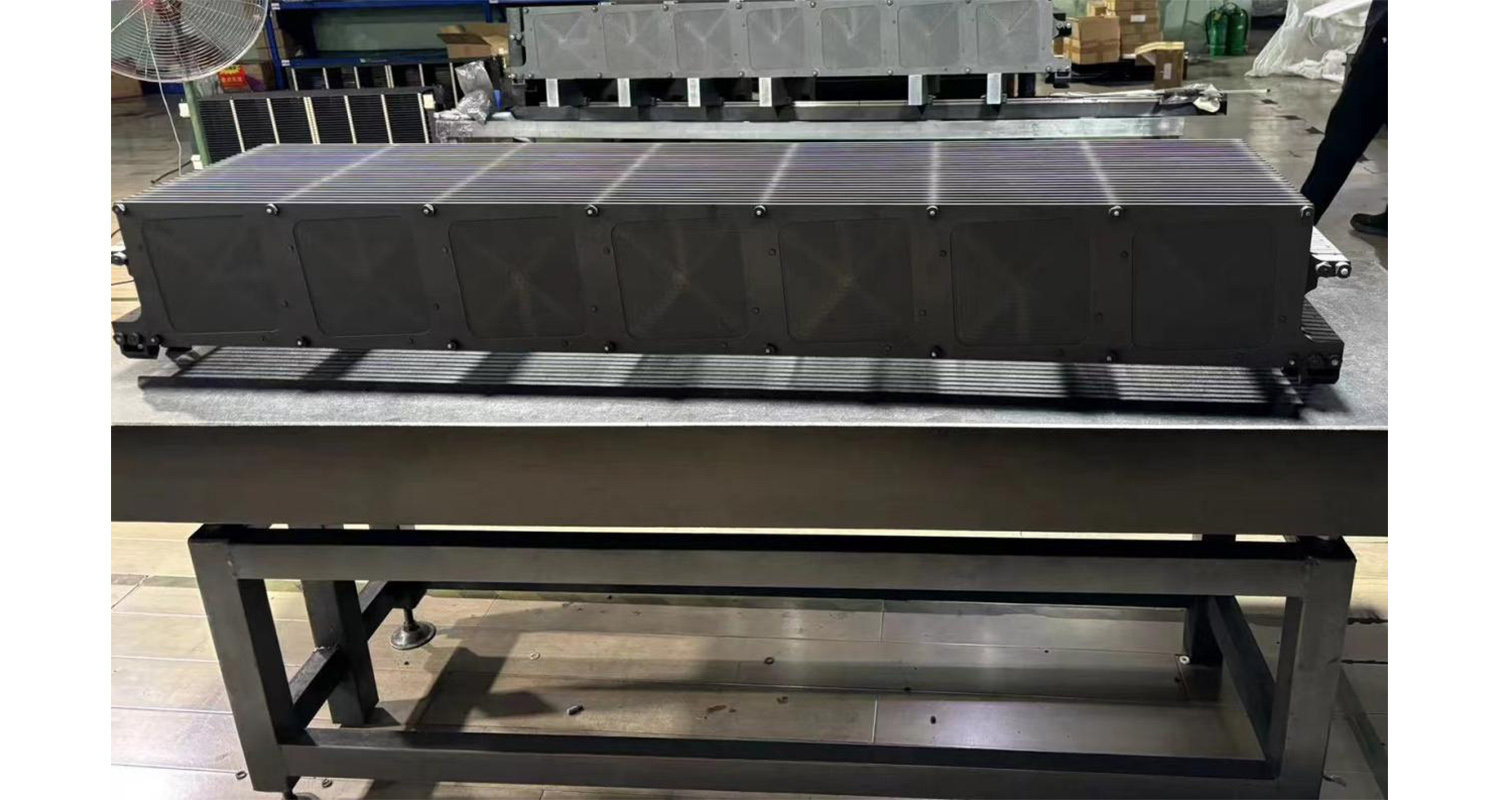
How to Specify PPB-Level Purity in Your Procurement
Key takeaway: A ppb-level purity specification is only as good as the verification behind it. Require batch-level ICP-MS and GDMS reports, and include an independent verification clause in the purchase contract.
Specifying ppb-level purity in a graphite boat purchase order requires more than just writing “semiconductor grade” on the spec sheet. Here‘s what to include.
1. Define the elements and limits. Specify boron ≤0.1 ppm, aluminum ≤0.1 ppm, total metallic <20 ppm, and individual transition metals <1 ppm. Reference SEMI C-001 as the baseline standard.
2. Require batch-level analysis. Don‘t accept a generic material certificate. Require ICP-MS and GDMS reports for each production batch of the graphite boat.
3. Specify the analytical method. Boron analysis should use GDMS. If the supplier only provides ICP-MS data, ask how they account for boron loss during sample preparation.
4. Include a verification clause. State that the buyer has the right to verify purity through independent laboratory testing. This is standard practice in semiconductor procurement.
5. Define the consequences. If a batch fails the purity specification, the supplier should replace it at no cost. The cost of a failed semiconductor crystal growth run — tens of thousands of dollars — far exceeds the cost of the boat itself.
Frequently Asked Questions
Q1: Why isn‘t ash content sufficient for semiconductor-grade graphite?
Ash content measures total non-carbon residue weight, but it doesn‘t identify which elements are present. A graphite sample with 5 ppm ash that‘s mostly boron is worse for semiconductor processing than one with 20 ppm ash that‘s mostly silicon. Boron is a p-type dopant that shifts crystal doping at ppb concentrations. You need elemental analysis to know what‘s actually in the graphite.
Q2: What‘s the difference between ICP-MS and GDMS?
ICP-MS dissolves the graphite sample in acid and analyzes the solution. GDMS analyzes the solid sample directly. The key difference for semiconductor applications: GDMS is better for boron analysis because boron can be lost during ICP-MS acid digestion. The standard practice is to require both methods for critical applications.
Q3: How do I know if a supplier‘s purity claims are accurate?
Ask for batch-level ICP-MS and GDMS reports. Look for boron specifically — it‘s the most critical element and the most difficult to control. If the supplier can‘t provide elemental analysis data, they‘re not a semiconductor-grade supplier. At VET Energy, we provide full elemental analysis with every semiconductor-grade boat shipment.
Q4: What happens if a graphite boat fails the purity specification after it‘s been installed?
The boat should be replaced immediately. Contaminated boats will continue to release impurities into the process until they‘re removed. The cost of one failed crystal growth run typically exceeds the cost of the boat itself, so there‘s no economic justification for continuing to use a non-compliant boat.
Q5: Can a ppb-level purity graphite boat be recycled or reused?
Graphite boats that have been used in semiconductor processing are generally not recycled back into semiconductor applications. The surface contamination and thermal history make it difficult to restore the material to the original purity specification. Used boats are typically downgraded to less demanding applications or recycled as raw material for lower-grade graphite products.
Summary and How VET Energy Can Help
Graphite boat contamination in semiconductor manufacturing is a ppb-level problem. Ash content specifications that work for PV applications are insufficient for semiconductor crystal growth, where boron and aluminum contamination at ppb concentrations can ruin an entire production run.
At VET Energy, we understand the purity requirements for semiconductor-grade graphite. We provide batch-level ICP-MS and GDMS analysis with every semiconductor-grade boat shipment, and we work with customers to define the right purity specification for their process. Dr. Wang our technical lead, has 12 years of experience in graphite component design for semiconductor and photovoltaic applications.
If you need graphite boats with verified ppb-level purity for SiC crystal growth or semiconductor epitaxy, contact us for a technical consultation. We‘ll provide the analytical data you need to make an informed decision.
References
- SEMI C-001 — Specification for High-Purity Graphite. SEMI International Standards. (Framework for metallic contamination limits)
- US Patent Application. “Vapor Deposition Apparatus and Techniques Using High Purity Polymer Derived Silicon Carbide.” 2023. (Boron content in commercially available graphite: typically above 0.2 ppm, up to 1 ppm)
- Mersen. “Ultra High Purity Graphite for Semiconductor Applications.” (Purity levels below 5 ppm for semiconductor-grade graphite)
- IndexBox. “Graphite Refractory Blocks Market Report.” 2026. (SEMI C-001 and OEM purity specifications for semiconductor applications)
Post time: Dec-23-2024